Buck Converter
Code for a controller of a Buck-type DC-DC source, based on the block diagram of a Step-Down Switching Regulator
Devices & Components
Arduino Nano
Resistor 4.75k ohm
1N4007 – High Voltage, High Current Rated Diode
Resistor 1k ohm
1N5819 – 1A Schottky Barrier Rectifier
Capacitor 220 µF
General Purpose Transistor NPN
Resistor 10k ohm
MOSFET Transistor, P Channel
Hardware & Tools
Cable Cutter, 143mm
Soldering iron (generic)
Solder Wire, Lead Free
Prototyping Kit, Breadboard
Project description
Code
Buck_converter.ino
c_cpp
You can use this code easily by changing the voltage to be regulated in the code. The conversion factor comes from the voltage divider used for feedback and its value is by: 1k / (1K + 4.7K)
1//*************************** Change these values at base of your needs
2  *****************************
3#define VoltageR 9.1f //Voltage to regulate
4
5//
6  Setup of mainboard **********************************************************
7#define
8  convertion 0.1754f //Conversion factor
9
10// Definition of inputs and outputs
11  ********************
12const int uPin = 9; // Control voltage, this is the pin
13  called OC1A
14const int x0Pin = A0;  //Voltage at the output of the second integrator
15
16//
17  Variables to signal feedback *************************
18float FB = 0; // Feedback
19  signal
20float RV = 0; // Reference Voltage
21int e = 0;    // Error variable
22float
23  Switch_cycle = 0; //Dute Cycle
24
25// Variables to time operations **************************
26unsigned
27  long softStart = 500;
28
29void setup() {
30
31  //******************** Set
32  all inputs and outputs **********************************************************
33
34  pinMode(uPin,OUTPUT); // Set pin OC1A as output
35  pinMode(13,OUTPUT);   //
36  To indicate the device is operate
37
38  //******************** Set and Clear
39  initial ***************************************************
40  digitalWrite(13,LOW);
41  // Start Led Off
42
43  //******************** Calculate all conversions **********************************************************
44
45  RV = (VoltageR*convertion*1024/5); //Convert voltage reference to conversion ADC
46  value
47
48  //******************* Delay before start operation ********************************************************
49
50  SoftStartDelay();
51
52  noInterrupts(); // disable all interrupts while
53  do configure
54  // ******************************* Set PWM frecuency **********************************************
55
56  // Freq_PWM = 16Mhz /128 = 125 Khz
57  TCCR1A = (1<<COM1A1) | (0<<COM1A0) |
58  (0<<COM1B1) | (0<<COM1B0) | (1<<WGM11) | (0<<WGM10);
59  //       COM1A1 = 1
60  ; COM1A0 = 0 ; COM1B1 = 0  ; COM1B0 = 0  ;         Note: When use a inverted output,
61  you must set COM1A1 & COM1A0, if you use a normal output, you only have to must
62  COM1A1
63  //       Clear output OC1A when match happen, Output OC1B disconnected
64
65  TCCR1B = (0<<ICNC1) | (0<<ICES1) | (1<<WGM13) | (1<<WGM12) | (0<<CS12) | (0<<CS11)
66  | (1<<CS10);
67
68  //        ICNC1 & ICES1 are used when Timer had a external
69  signal. Unused in Fast PWM mode
70  //        CS12 = 0; CS11 = 0; CS10 = 0; Select
71  no prescaler
72  //        WGM13 = 1 ; WGM12 = 1;  WGM11 = 1 ; WGM10 = 0; Select
73  Fast 8 bit PWM with TOP value on ICR1
74
75  ICR1H  = 0x00;  //Set ICR1 register
76  to 80h (#128) MSB = 0x00, LSB = 80h
77  ICR1L  = 0x80;  //This value is TOP of
78  the counter. Timer reach to zero when count is equal to it.
79
80  TCNT1H =
81  0x00; //Reset MSB of the timer
82  TCNT1L = 0x00; //Reset LSM of the timer
83
84  OCR1AH = 0x00; //Clear MSB of the match register, unused in Fast PWM 8 bit
85
86  OCR1AL = 0x00; //Set zero to start device off, it register is used to change dute
87  cycle
88
89  // ****************************** Set interrup by timer 2 ******************************************
90
91  // T = (1/16MHz)*(2^8-00)*8 = 128 uS
92  TCCR2A = (0<<COM2A1) | (0<<COM2A0) |
93  (0<<COM2B1) | (0<<COM2B0) | (0<<WGM21) | (0<<WGM20);
94  //       COM1A1 = 0
95  ; COM1A0 = 0  ; COM1B1 = 0  ; COM1B0 = 0  ;
96  //       OC12A and OC2B both
97  are disconnected
98
99  TCCR2B = (0<<WGM22) | (0<<CS22) | (1<<CS21) | (0<<CS20);
100
101  //        CS22 = 0; CS21 = 1; CS20 = 0; Select prescaler Fosc/8
102  //        WGM13
103  = 0 ; WGM12 = 0;  WGM11 = 0 ; WGM10 = 0; Select Normal Mode operation
104
105  TCNT2
106  = 0x00; //This register have a pre-load of the timer. However, in this case, it's
107  no have pre-load
108  OCR2A = 0x00; //Clear match register. It's unused
109  OCR2B
110  = 0x00; //Clear match register. It's unused
111
112  TIMSK2 = (0<<OCIE2B) | (0<<OCIE2A)
113  | (1<<TOIE2); // enable timer2 overflow interrupt
114  // ******************************
115  End of the configurate *******************************************
116  interrupts();
117  // enable all interrupts
118}
119ISR(TIMER2_OVF_vect) // interrupt service routine
120
121{
122  FB = (float)(analogRead(x0Pin));          //Feedback signal
123
124  float
125  k = 0.08;                           //Gain in close loop
126  e = RV-FB;                                //Error
127
128  Switch_cycle = Switch_cycle + e*k;        //Control
129  if(Switch_cycle<=0)                       //Min
130  duty Cycle = 0
131    Switch_cycle = 0;
132  if(Switch_cycle>=122)                     //Mx
133  duty Cycle = 95% ;(122/128)*100 = 95.31% real value
134    Switch_cycle = 122;
135
136    OCR1AL = (unsigned char)(Switch_cycle); //Write duty cycle
137}
138void SoftStartDelay()
139  // Delay with interval of 500ms before start regulation
140{
141  delay(softStart);
142
143  digitalWrite(13,HIGH);
144}
145void loop() {
146  // put your main code here,
147  to run repeatedly:
148
149}
150
Buck_converter.ino
c_cpp
You can use this code easily by changing the voltage to be regulated in the code. The conversion factor comes from the voltage divider used for feedback and its value is by: 1k / (1K + 4.7K)
1//*************************** Change these values at base of your needs  *****************************
2#define VoltageR 9.1f //Voltage to regulate
3
4//  Setup of mainboard **********************************************************
5#define  convertion 0.1754f //Conversion factor
6
7// Definition of inputs and outputs  ********************
8const int uPin = 9; // Control voltage, this is the pin  called OC1A
9const int x0Pin = A0;  //Voltage at the output of the second integrator
10
11//  Variables to signal feedback *************************
12float FB = 0; // Feedback  signal
13float RV = 0; // Reference Voltage
14int e = 0;    // Error variable
15float  Switch_cycle = 0; //Dute Cycle
16
17// Variables to time operations **************************
18unsigned  long softStart = 500;
19
20void setup() {
21
22  //******************** Set  all inputs and outputs **********************************************************
23  pinMode(uPin,OUTPUT); // Set pin OC1A as output
24  pinMode(13,OUTPUT);   //  To indicate the device is operate
25
26  //******************** Set and Clear  initial ***************************************************
27  digitalWrite(13,LOW);  // Start Led Off
28
29  //******************** Calculate all conversions **********************************************************
30  RV = (VoltageR*convertion*1024/5); //Convert voltage reference to conversion ADC  value
31
32  //******************* Delay before start operation ********************************************************
33  SoftStartDelay();
34
35  noInterrupts(); // disable all interrupts while  do configure
36  // ******************************* Set PWM frecuency **********************************************
37  // Freq_PWM = 16Mhz /128 = 125 Khz
38  TCCR1A = (1<<COM1A1) | (0<<COM1A0) |  (0<<COM1B1) | (0<<COM1B0) | (1<<WGM11) | (0<<WGM10);
39  //       COM1A1 = 1  ; COM1A0 = 0 ; COM1B1 = 0  ; COM1B0 = 0  ;         Note: When use a inverted output,  you must set COM1A1 & COM1A0, if you use a normal output, you only have to must  COM1A1
40  //       Clear output OC1A when match happen, Output OC1B disconnected
41  TCCR1B = (0<<ICNC1) | (0<<ICES1) | (1<<WGM13) | (1<<WGM12) | (0<<CS12) | (0<<CS11)  | (1<<CS10);
42
43  //        ICNC1 & ICES1 are used when Timer had a external  signal. Unused in Fast PWM mode
44  //        CS12 = 0; CS11 = 0; CS10 = 0; Select  no prescaler
45  //        WGM13 = 1 ; WGM12 = 1;  WGM11 = 1 ; WGM10 = 0; Select  Fast 8 bit PWM with TOP value on ICR1
46
47  ICR1H  = 0x00;  //Set ICR1 register  to 80h (#128) MSB = 0x00, LSB = 80h
48  ICR1L  = 0x80;  //This value is TOP of  the counter. Timer reach to zero when count is equal to it.
49
50  TCNT1H =  0x00; //Reset MSB of the timer
51  TCNT1L = 0x00; //Reset LSM of the timer
52  OCR1AH = 0x00; //Clear MSB of the match register, unused in Fast PWM 8 bit
53  OCR1AL = 0x00; //Set zero to start device off, it register is used to change dute  cycle
54
55  // ****************************** Set interrup by timer 2 ******************************************
56  // T = (1/16MHz)*(2^8-00)*8 = 128 uS
57  TCCR2A = (0<<COM2A1) | (0<<COM2A0) |  (0<<COM2B1) | (0<<COM2B0) | (0<<WGM21) | (0<<WGM20);
58  //       COM1A1 = 0  ; COM1A0 = 0  ; COM1B1 = 0  ; COM1B0 = 0  ;
59  //       OC12A and OC2B both  are disconnected
60
61  TCCR2B = (0<<WGM22) | (0<<CS22) | (1<<CS21) | (0<<CS20);
62  //        CS22 = 0; CS21 = 1; CS20 = 0; Select prescaler Fosc/8
63  //        WGM13  = 0 ; WGM12 = 0;  WGM11 = 0 ; WGM10 = 0; Select Normal Mode operation
64
65  TCNT2  = 0x00; //This register have a pre-load of the timer. However, in this case, it's  no have pre-load
66  OCR2A = 0x00; //Clear match register. It's unused
67  OCR2B  = 0x00; //Clear match register. It's unused
68
69  TIMSK2 = (0<<OCIE2B) | (0<<OCIE2A)  | (1<<TOIE2); // enable timer2 overflow interrupt
70  // ******************************  End of the configurate *******************************************
71  interrupts();  // enable all interrupts
72}
73ISR(TIMER2_OVF_vect) // interrupt service routine
74{
75  FB = (float)(analogRead(x0Pin));          //Feedback signal
76
77  float  k = 0.08;                           //Gain in close loop
78  e = RV-FB;                                //Error
79  Switch_cycle = Switch_cycle + e*k;        //Control
80  if(Switch_cycle<=0)                       //Min  duty Cycle = 0
81    Switch_cycle = 0;
82  if(Switch_cycle>=122)                     //Mx  duty Cycle = 95% ;(122/128)*100 = 95.31% real value
83    Switch_cycle = 122;
84    OCR1AL = (unsigned char)(Switch_cycle); //Write duty cycle
85}
86void SoftStartDelay()  // Delay with interval of 500ms before start regulation
87{
88  delay(softStart);
89  digitalWrite(13,HIGH);
90}
91void loop() {
92  // put your main code here,  to run repeatedly:
93
94}
95
Downloadable files
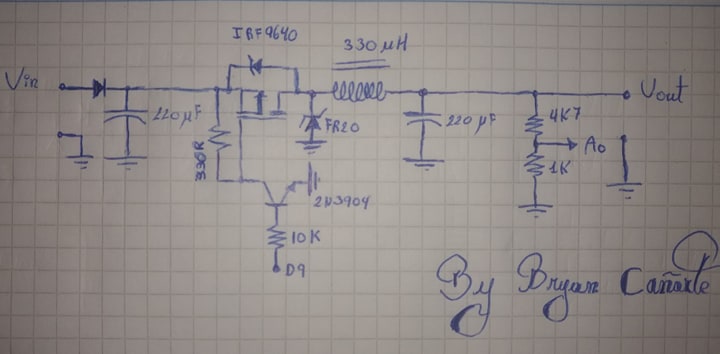
Schematic
Connect the signal marked d9 and A0 to the pins of the same name of the arduino. The MOSFET and high speed diode can be exchanged for similar components.
Schematic
Comments
Only logged in users can leave comments